
To print some of the smallest features on a chip, ASML starts by destroying a droplet of tin.
A laser pulse flattens it. A stronger pulse turns it into plasma. The plasma gives off light, including the extreme ultraviolet that the machine needs. A set of mirrors catches a small share of that light and sends it towards a silicon wafer. Then another droplet arrives. In the established source design ASML describes, this happens 50,000 times a second. How the light is made ↗
That is an unreasonable amount of work for a lamp.
Veritasium's tour of ASML ↗ spends nearly an hour explaining why it is necessary. The machinery is wonderful to look at. But the interviews are better. The engineers keep describing a problem they solved, then mentioning what went wrong because they had solved it. More light meant more heat. Tin made a good light source and a terrible neighbour for a clean mirror.
I want to understand that part. We have a familiar way of telling the history of computing: smaller transistors, faster chips, another generation. It leaves out the people trying to stop a mirror getting dirty.
Why the light had to change
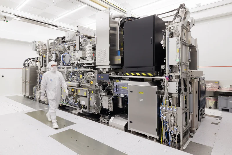
Lithography transfers a pattern onto a wafer coated in a light-sensitive material called photoresist. Exposure changes the resist's chemistry. Development leaves selected areas protected and others open, allowing later steps to etch or otherwise modify the material beneath. This happens repeatedly as the chip's structures and connections are built up. An EUV machine does the exposure; it doesn't make an entire processor by itself. How chips are made ↗
Light decides what stays.
- Coat
A light-sensitive resist covers the material to be patterned.
- Expose
The image changes the chemistry of selected areas.
- Develop
Exposed resist is removed, opening a pattern.
- Transfer
Etch the exposed film, then strip the remaining resist.
The difficulty is that light doesn't draw perfectly sharp edges. It diffracts. Make the pattern fine enough and features that should be separate become hard to distinguish.
Chipmakers had already pushed deep ultraviolet light remarkably far. The familiar 193 nm wavelength can produce features much smaller than 193 nm, using sophisticated optics and manufacturing techniques. There is no rule saying you can't print below one wavelength. But squeezing more out of the same light becomes expensive. Some patterns need to be split across several manufacturing steps, each with another opportunity for error.
EUV takes the wavelength down to 13.5 nm. That buys resolution, at the cost of replacing much of the machine that made the old approach practical. Ordinary lenses absorb it. Air absorbs it. The mask carrying the circuit pattern has to reflect it. You now need a largely evacuated light path and an optical system built around specialised mirrors. DUV remains useful for other layers, including in chips that use EUV. The two systems ↗
A smaller wavelength helps. So does a wider aperture.
- CD
- Smallest printed feature in this model
- λ
- Wavelength of the light
- NA
- How wide an angle the optics collect
- k1
- Factor describing the process
Hold λ at 13.5 nm and use an illustrative k1 = 0.32. Increasing NA from 0.33 to 0.55 reduces the calculated feature size by 40%.
The equation makes the attraction clear. Reduce the wavelength and, with everything else held fixed, you can print a smaller feature. But the equation doesn't include a term for how miserable the new wavelength will be to work with.
You need a source and a mirror that agree
Why 13.5 nm? Why not go even shorter?
You have to produce enough light at a wavelength you can also reflect. Tin plasma emits strongly around 13.5 nm. Alternating layers of molybdenum and silicon make a useful mirror in that same neighbourhood. These two facts fit together. Picking the shortest wavelength on a chart would have been much easier.
The mirrors are a lovely piece of physics. A little of the incoming wave reflects at each interface in the coating. The layer thicknesses are chosen so that those reflections reinforce one another at the intended wavelength. It is a carefully made stack, deposited on an extraordinarily precise surface. ZEISS on EUV optics ↗
Small reflections add up.
The surface carries alternating thin layers of two materials.
Reflections from the interfaces reinforce one another around the wavelength the coating was designed for.
Some light is still absorbed.
Even a good EUV mirror loses a substantial fraction of the light. Suppose each reflection keeps 70%. After seven reflections, about 8% remains. After nine, about 4%. These are illustrative paths, not the complete optical budget of a particular scanner. The arithmetic alone explains why making a little EUV was never enough.
Where did the light go?
remains after 7 reflections
at 70% reflectivity per reflection.
R = 0.70 for every reflection. N is the number of reflections. Other optical and source losses are excluded.
Removing mirrors would help with the losses. Unfortunately, the mirrors also have jobs: shaping the illumination, reducing the image, correcting distortions. Take one away and you may get more light in the wrong places.
The tin target needed work too. Hitting a compact droplet wastes energy and can let the tin reabsorb some of the light you wanted. A preparatory pulse spreads the droplet out before the main pulse arrives. Its shape becomes part of the light-source design. The video describes newer work with an additional pulse; the basic two-pulse sequence below is the established version explained in ASML's public overview.
First, change the shape of the tin.
- Droplet
A small, repeatable target.
- Pre-pulse
Spread out the tin.
- Main pulse
Create the emitting plasma.
The next droplet must arrive where the laser expects it. The pulse must change its shape in a useful way. The main pulse must catch it at the right moment. And the debris from this event must leave the next one possible.
The mirror has to survive its light source
There is something almost comical about putting a surface this carefully made next to exploding metal.
Tin debris can contaminate the collector, the mirror closest to the plasma. As its reflectivity falls, less useful light reaches the rest of the machine. You can stop and clean it. A factory owner would prefer you didn't need to do that very often.
Hydrogen helps slow debris and remove deposited tin through chemical reactions. But gas in the chamber also absorbs light, and energy from the plasma heats it. Its flow and pressure need to be managed along with everything else. The source is simultaneously an optics problem, a plasma problem and a cleaning problem. Research on EUV sources ↗
In the interviews, an engineer describes using an ultrafast camera to understand blast waves travelling through the hydrogen after each plasma event. Someone had to work out where that energy was going. Elsewhere in the story, opening the machine appeared to improve the collector's condition. That observation led the team to experiment with adding a little oxygen. Imagine spending years keeping air out of a machine, then discovering that letting some of it in had helped. The source and collector interviews ↗
The problems share a chamber.
More useful EUV. More energy and debris to manage.
Hydrogen helps with debris and cleaning.
Absorption and gas heating become part of the problem.
Balance cleaning, cooling and light transmission.
The precision problem continues at the wafer. Each new pattern has to line up with what is already there. A beautifully printed layer in the wrong place can still ruin the device.
And the wafer has to move. Holding everything still would make some measurements easier, but a scanner has to expose many fields across many wafers. ASML's twin-stage arrangement measures one wafer while another is being exposed. Position sensing and correction happen continuously; precision is something the operating machine keeps maintaining. Mechanics and measurement ↗
The next layer must land in the right place.
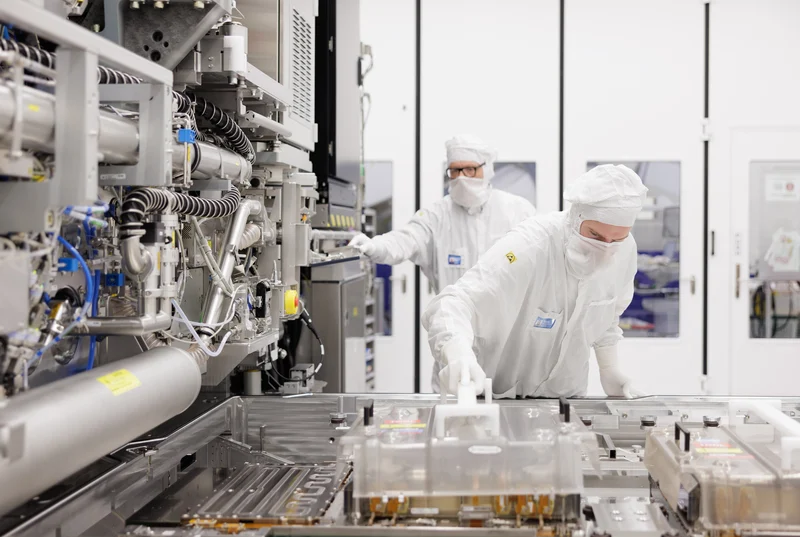
That changes how I picture the machine. I tend to imagine precision as a property of an object: a straight edge, a smooth surface, a part cut to the right size. Here, the temperature changes and the stages move. Measurements have to keep catching the difference between where things are and where they should be.
When was EUV finished?
By April 2001, a collaboration involving three US national laboratories and a semiconductor-industry consortium had an EUV Engineering Test Stand. The announcement already described the technology as a route to future chip production. You can read it now, with the benefit of knowing how much work remained. The 2001 announcement ↗
Hiroo Kinoshita had demonstrated EUV imaging in Japan in the 1980s. The laboratory teams developed optics and measurement techniques that industry would need. ASML, ZEISS, the light-source company Cymer and many others then had to turn those capabilities into equipment a chipmaker could use. ASML's own history describes years of missed targets and source-power problems. From lab to fab ↗
The dates are years apart.
- EUV images
Kinoshita's early imaging work.
- Engineering Test Stand
A laboratory and industry prototype.
- Demo tools ship
Researchers can develop processes on EUV equipment.
- Pre-production system
The NXE:3100 reaches a customer.
- Production system ships
The NXE:3300 is another step, with work still ahead.
- Orders grow
Customers order the NXE:3400 in greater numbers.
A working prototype answered a serious question: can we form the image? It left several expensive questions open.
- How many wafers can it expose in an hour?
- How much of the week will it spend waiting for maintenance?
- Do the layers line up after the machine has warmed up?
- Can the customer repeat the result without the development team standing beside it?
Those questions also make it difficult to choose a sensible moment to give up. If the source power is improving but the collector keeps failing, are you getting close? Or have you built a machine whose parts cannot work together at the required pace?
It is easy to answer after EUV succeeds. Before that, someone has to pay for the next experiment. The alternative technology is improving in the meantime, so yesterday's target may no longer be good enough. In 2012, Intel, TSMC and Samsung joined ASML's customer co-investment programme to help fund the next stage of development. The companies that needed better chips also needed the equipment supplier to survive the work. The completed programme ↗
Left there with the machine
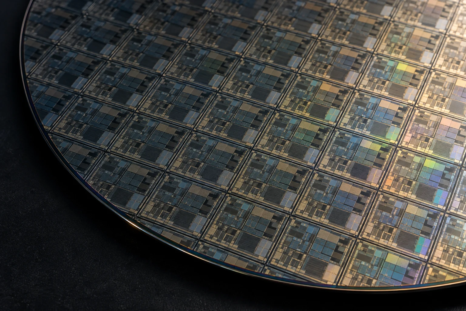
I keep wondering how much of this work disappears from the finished product. You can look up the wavelength and the resolution. It is harder to see the failed tests that taught someone which measurement to distrust, or why a seemingly minor change was abandoned. Buying the parts would leave you with years of that learning to do.
Near the end of the Veritasium video, Jos Benschop recalls seeing an early system installed at a customer's fab in 2010. For him, that was the moment the bet felt justified. Years later, he met the person who had helped install it. After Benschop had gone home, the machine broke down. Getting it running again took two months.
I like that they left both versions in. One person remembers the machine finally standing in the customer's factory. The other remembers being left there with it.