Robust and fragile at the same time
On the outskirts of Taichung, across the road from a few rice farms, sits one of the most important buildings in the world. It is a 30,000 m² DRAM mega-campus where billion-dollar lithography machines run around the clock. The memory coming off that line ends up in military gear, network infrastructure, and most lucratively the enterprise GPUs that run data centers.
Here is the thing that got me. The chips leaving that fab aren't even finished yet. And they are already the output of more than 6,000 suppliers across 40+ countries. Machines that make the machines that make the machines.
This supply chain is way more robust than people think, and way more fragile. Both at once.
That sounds like a contradiction. It isn't. The chain is robust because every single node is run by specialists who spent decades getting unbeatably good at one narrow thing. It is fragile for the exact same reason. Being that good is precisely why there is usually only one of them. The only way I could make sense of it was to start at the bottom, with raw elements, and climb.
One ziggurat, narrowing all the way up
Read this one bottom to top. At every layer up, the number of suppliers who can actually do the job collapses. The base is commodity stuff anyone can buy. The top is single companies that hold the whole world to ransom on know-how alone. Notice that the chip designers don't sit in the stack at all. They feed blueprints in from the side.
The toilet company that holds up Moore's Law
On the Japanese island of Kyushu, a ceramics maker presses ultra-pure aluminium oxide and a classified blend of other materials into the most uniform ceramic plates anyone alive knows how to make. The whole trick is that the material barely expands when heated, and it's diamagnetic.
Why care? You've seen the footage of a silicon wafer getting flung back and forth inside a sealed chamber hundreds of times a minute. Turns out just holding that wafer still is its own nightmare.
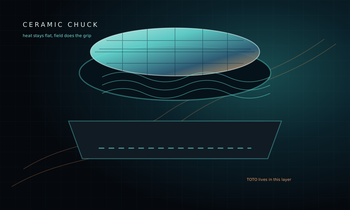
A chuck the size of a dinner plate costs six figures, and that's before the multi-million-dollar machine it plugs into. And TOTO isn't even the only unexpected monopolist hiding in here.
The MSG company under your CPU
Ajinomoto, the company that gave the world monosodium glutamate, took its organic-chemistry expertise and made ABF (Ajinomoto Build-up Film), the thin insulating film that sits under almost every advanced chip on earth. It's a stable dielectric, you can pattern it at fine pitch, and it takes copper plating unusually well. Nobody has credibly matched it.
The substrate under your GPU is layers of that film with copper traces drilled through it by thousands of microscopic vias. That layer count has crept from four up to well over a dozen on a modern accelerator. Those substrates then get assembled by another tiny club, mostly Ibiden and Unimicron.
Two of the hardest choke points in all of computing aren't chip companies. One makes ceramics, the other makes a food additive. Both spent fifty years getting freakishly good at a process that happened to sit right next to what the industry suddenly needed. Nobody designed these monopolies. They accreted. The moat here is depth of craft, not strategy, and you can't shortcut your way to it.
How ASML boils tin to print atoms
Inside the fab, the lithography machine gets all the attention, and one name owns it: ASML, the Dutch company spun out of a 1984 Philips venture. A single machine carries over 5,000 of its own suppliers. TRUMPF lasers from Germany. Zeiss optics polished to single-atom smoothness. Power supplies steadier than the ones running a hospital. Vacuum pumps that knock atoms out one at a time.
The most advanced units are so large ASML ships them in pieces aboard three Boeing 747s, with an army of engineers who spend weeks rebuilding the machine on the factory floor. Here is what actually happens inside the cutting-edge TWINSCAN NXE:3800E when it fires:

The myth of the single lithography company
You may have heard ASML is the only company making these machines. Not quite. Nikon and Canon, the camera people, build them too. ASML's real distinction is narrower than that. It alone can build the bleeding-edge EUV machine. The others sit a generation back on resolution, and here's the catch most coverage misses: that mostly doesn't matter.
Most chips on Earth are perfectly happy a generation behind.
Toasters, Wi-Fi routers, hospital monitors, washing machines, your latest vaccine. None of these mass-market chips need the leading edge. They run fine on older Canon and Nikon tools. And since the US has export-controlled ASML even though it isn't American, any buyer who doesn't strictly need the frontier often just buys a simpler machine and skips the diplomatic paperwork entirely. A basic lithography unit costs barely more than a loaded pickup truck.
The easy mistake in hardware is assuming you need the frontier node. The frontier gets the headlines and the geopolitics. The volume and the margin usually live a node or two back. Pick the node your product actually needs, not the one that sounds impressive. Cutting edge is a cost center until the workload genuinely demands it.
Lithography is one station on a long line
An EUV scanner without the rest of the fab is, to borrow a good line, a very expensive laser pointer. Building a chip means cycling a wafer through deposition, coating, lithography, etch, polish and inspection more than a dozen times. Five companies own those stations, and each one is the undisputed leader of its own.
Three of the five are American, which keeps them out of the headlines that hound the more exposed Dutch ASML, and makes regulators far less likely to poke at companies they've never heard of. The low profile is partly the point.
Why you can't just rebuild it
Any country that wanted full independence from this chain would have to rebuild all five toolmakers plus their thousands of suppliers. That's a project measured in decades, if it's possible at all. A lot of these firms were sharpening their industrial processes before modern silicon even existed. Starting from fundamentals is a very different thing from reverse-engineering some machinery.
You can buy the machines. The decades of tacit skill that make them produce anything useful, you cannot.
Four factories, one nine-tenths
All of those tools flow into just four companies: Samsung, GlobalFoundries, Intel and above all TSMC. With Intel's exception, they don't design the chips. They manufacture other firms' designs. Picture Ford designing the Focus and then handing the entire build to a factory that is also assembling a competitor's Corolla on the same floor. It's odd, but the skill and the capital are so concentrated that doing it in-house makes no sense for anyone who wants to ship this decade.
The "T" stands for Taiwan, which sits squarely in Beijing's crosshairs. There's a framing I can't improve on: it's the Strait of Hormuz, except 80% of the world's oil flows through it instead of 20%, the oil is made of glass, and we've built the most concentrated pool of investment in history on top of that glass.
Under US pressure, TSMC is building fabs in Arizona and Japan. But the most advanced node is still made almost entirely at home, and TSMC openly admits the overseas sites run a generation or two behind, with Arizona in particular hitting repeated delays and cost overruns. It isn't a tooling problem. The tools are available. The part you can ship on paper isn't the bottleneck. The tacit craft is.
Sand, memory, and advanced packaging
Before any foundry can start, it needs bare 300 mm wafers, and two Japanese firms, Shin-Etsu and Sumco, supply roughly half the global market between them. GlobalWafers in Taiwan and Siltronic in Germany hold the smaller slices. Quartz sand gets refined into polysilicon so pure that contamination is counted in parts per billion, then melted and pulled into a single crystal by the Czochralski process, then sliced and polished. A hiccup at any step ripples through every fab on the planet. In 2021 a fire at one Shin-Etsu supplier helped trigger a global chip shortage that left half-finished cars parked on dealer lots for nearly two years.
The memory nobody else can package
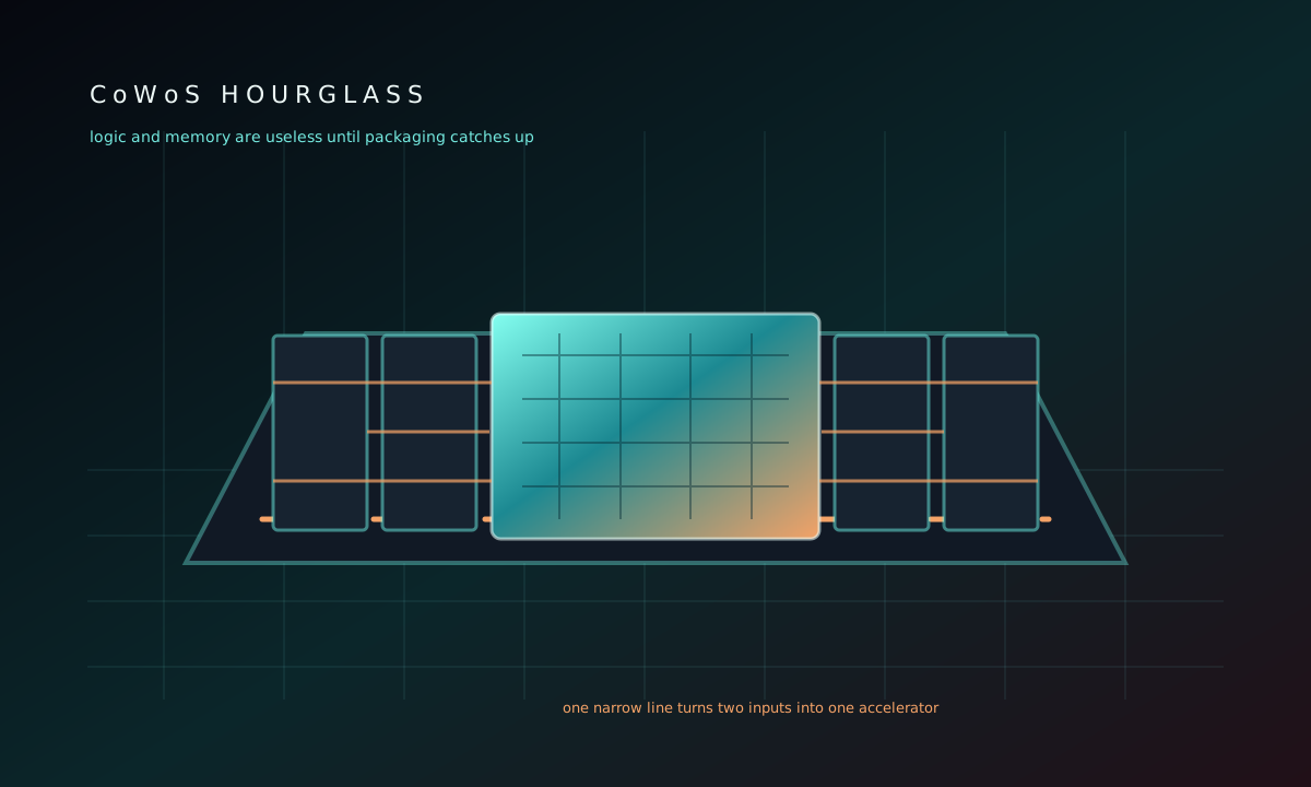
Logic is only half the story. Without DRAM, and increasingly without stacks of high-bandwidth memory (HBM) sitting right next to the GPU, even the best logic chip is useless because it has nothing to read from or write to fast enough to matter. Samsung does both logic and memory. SK Hynix and Micron are the dedicated memory leaders. Together the three of them supply basically 100% of the serious market.
SK Hynix has become the sole qualified supplier of the most advanced HBM3e stacks Nvidia bolts onto its top accelerators. So the entire AI boom is sitting on memory designed in Incheon and packaged with bonding-wire processes that almost nobody outside South Korea can run at volume. And the tightest knot of the whole thing is still one step further on.
The software that draws what doesn't exist yet
Nvidia, Apple, AMD, Broadcom and Qualcomm don't manufacture their chips, and they don't design them with their own tools either. Drawing a modern chip means modeling tens of billions of transistors while working out how they'll behave at a scale where quantum uncertainty is a real engineering input rather than a curiosity. Two companies sell that software competitively: Cadence and Synopsys.
A ten-engineer team can burn several million dollars a year just on licenses, and they pay it because there's no replacement. Switching would mean rebuilding the entire design pipeline on tools nobody they trust has ever shipped on. Both companies are American, so Washington can, and has, added their software to the export-control list. The verification layer the whole industry stands on is two companies wide.
Why the monopolies don't run riot
This was a narrow slice. I barely touched JSR and Tokyo Ohka's photoresist, Air Liquide and Linde's specialty gases, Hoya's mask blanks, Tanaka's bonding wire, or the subsystem makers buried two and three levels deep inside a single EUV scanner's bill of materials. Hyper-specialization at the edge of what's scientifically possible leaves single points of failure everywhere. It also leaves a set of firms that have gotten extraordinarily good at working together, because there's genuinely nowhere else for any of them to go.
So as long as that holds, every new data center coming online keeps bidding up the price of ultra-pure aluminium oxide, MSG-grade organic chemistry, Zeiss-grade glass, Korean memory packaging, Taiwanese substrate capacity, and, while we're at it, the world's finest Japanese toilets.
Robustness and fragility here are the same fact wearing two faces. The chain holds because every link is run by the one specialist nobody can match. It's brittle for that identical reason, because there's only one of them. Being that good is exactly what makes them impossible to replace, and impossible to replace is just risk with better branding. That tension never resolves. It only gets priced. You feel a small version of it the first time you ship anything physical and realize one vendor quietly owns your roadmap.